Test Research, Inc. (TRI), a provider of test and inspection systems for the electronics manufacturing industry, will be participating in SEMICON Taiwan at the Taipei Nangang Exhibition Centre, Hall 1 – 4F, from 4-6th September 2024.
Joining TRI at booth #N0990 will be OmniMeasure, TRI’s SEMI inspection partner.
Attendees visiting TRI’s booth will have the opportunity to explore AI-powered Automated Optical Inspection (AOI) solutions tailored for the Semiconductor and Advanced Packaging Industry. TRI offers comprehensive SEMI Inspection solutions for Advanced Wafer Level Packaging (WLP), Panel Level Packaging (PLP), and SEMI Back-End Package processes.
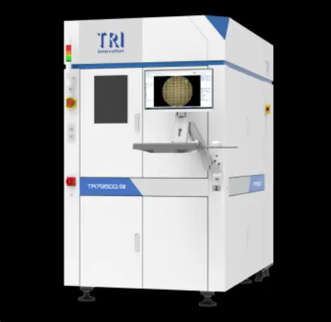
One of the highlights of TRI’s exhibition will be the new Wafer Inspection Platform, TR7950Q SII. This platform features a 25MP camera with 2.5μm resolution and a 12MP camera with a 0.55μm microlens, enabling high-resolution 2D/3D Defect-Free (DFF) inspection with AI-powered algorithms. The TR7950Q SII is designed for detailed Wafer Macroscopic 3D Inspection and precise micro measurement metrology. It can efficiently inspect Advanced WLP, Wafer Frames, Patterned Wafers, Wafer Bumping, Wafer Level Chip Scale Packages (WLCSP), and through-silicon vias (TSV). Thanks to the TSV module from OmniMeasure, the TR7950Q SII can perform ultra-high-speed TSV inspections, including measuring TSV depth, trench depth, and film thickness of oxide, nitride, PR, and PI.
In addition to the TR7950Q SII, TRI will showcase its latest back-end inspection solutions, the TR7007Q SII-S and TR7700Q SII-S. The TR7007Q SII-S is adept at inspecting Mini-LEDs, C4 bumps (~100μm diameter), and 008004 paste applications. The AI-powered 3D SEMI AOI, TR7700Q SII-S, can handle inspections of die, wire diameters up to 15μm (0.6 mil), System-in-Package (SiP), underfill, bumps, and more. The exhibit will also feature an X-ray Inspection Demo Station, demonstrating TRI’s SEMI AXI solutions for inspecting C4 bumps and copper pillars.
OmniMeasure will present its TGV (Through Glass Via) 3D Viewer, a metrology tool that uses non-contact tomography to provide clear cross-sectional views of glass vias. The TGV viewer also measures side wall angles without the need for Scanning Electron Microscopy (SEM).
Join TRI at Booth No. N0990 at SEMICON Taiwan 2024 to discover TRI’s latest SEMI applications and cutting-edge inspection innovations for the Semiconductor and Advanced Packaging Industry.
Original article source:
https://www.electronicspecifier.com/news/events-news/tri-to-display-new-wafer-inspection-and-metrology-solution
FAQ
- What is the new TRI Wafer Inspection and Metrology Solution?
The new TRI Wafer Inspection and Metrology Solution is an advanced system designed for inspecting semiconductor wafers. It integrates high-resolution imaging, precise metrology, and AI-driven defect analysis to ensure high yield and quality in semiconductor manufacturing.
- What technologies are used in this solution?
The solution leverages advanced optics, AI-driven algorithms, and high-precision metrology to detect and measure defects on wafers. It combines optical inspection, 3D metrology, and machine learning to deliver comprehensive analysis and accurate measurements.
- What types of wafers can this system inspect?
The system is designed to inspect a wide range of semiconductor wafers, including silicon, gallium arsenide (GaAs), silicon carbide (SiC), and other materials used in the production of microelectronics, power devices, and photonics.
- How does the system improve defect detection?
The system improves defect detection through its AI-powered image analysis, which can identify and classify defects with high accuracy. Additionally, its high-resolution imaging allows for the detection of even the smallest defects, ensuring that only wafers meeting the highest quality standards proceed to the next stage of manufacturing.
- What are the key benefits of using TRI’s Wafer Inspection and Metrology Solution?
High Accuracy: Provides precise measurement and defect detection to improve yield.
Increased Throughput: Optimized for high-speed inspection, reducing bottlenecks in production.
AI Integration: Uses machine learning to continuously improve inspection accuracy.
Versatility: Can inspect various wafer types and sizes, adapting to different manufacturing needs.
Comprehensive Reporting: Offers detailed analytics and reporting tools to help manufacturers understand defect trends and improve process control.
- How does this solution integrate with existing manufacturing processes?
The TRI Wafer Inspection and Metrology Solution is designed to easily integrate with existing semiconductor manufacturing processes. It supports various automation protocols and can be customized to fit specific production environments, ensuring seamless operation alongside other equipment.
- What kind of support and training does TRI offer for this solution?
TRI provides comprehensive support and training for its wafer inspection and metrology solution, including on-site installation, operator training, and ongoing technical support. TRI also offers software updates and upgrades to ensure that the system remains at the cutting edge of technology.