Electronic waste, commonly known as e-waste, represents an escalating global challenge, with projections indicating it will worsen as new flexible electronics for robotics, wearable devices, health monitors, and other innovative applications, including single-use devices, continue to be developed.
Researchers at MIT, the University of Utah, and Meta have created a new type of flexible substrate material that offers a potential solution to this problem. This material not only facilitates the recycling of components and materials once a device reaches the end of its life but also allows for the scalable production of more intricate multilayered circuits than those currently available.
This innovative material is detailed in the journal RSC Applied Polymers, in a paper authored by MIT Professor Thomas J. Wallin, University of Utah Professor Chen Wang, and seven other researchers.
Wallin, an assistant professor in MIT’s Department of Materials Science and Engineering, commented on the broader issue:
“We recognize that electronic waste is an ongoing global crisis that’s only going to get worse as we continue to build more devices for the internet of things, and as the rest of the world develops.”
Historically, academic efforts have concentrated on developing alternatives to conventional flexible electronic substrates, which are typically made from a polymer known as Kapton—a trade name for polyimide.
While much research has focused on creating entirely new polymer materials, Wallin emphasised that this approach often overlooks the practical reasons for the original choice of materials:
“That really ignores the commercial side of it, as to why people chose the materials they did to begin with.” Kapton has been widely used due to its excellent thermal and insulating properties and the readily available source materials.
The global market for polyimide is projected to reach $4 billion by 2030. “It’s everywhere, in every electronic device basically,” Wang explained, referring to components like the flexible cables that connect different parts inside devices such as mobile phones or laptops. Its high heat tolerance also makes it popular in aerospace applications. Despite its widespread use, Wang noted: “It’s a classic material, but it has not been updated for three or four decades.”
However, Kapton’s resilience comes at a cost. Its resistance to melting or dissolving renders it difficult to reprocess, and its use in advanced architectures like multilayered electronics is hindered by the slow manufacturing process, which involves heating the material to between 200 and 300 degrees Celsius over several hours.
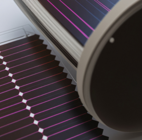
The alternative material developed by the research team, which is also a form of polyimide, offers compatibility with existing manufacturing infrastructure. This material is a light-cured polymer, similar to those used by dentists for durable fillings that harden within seconds under ultraviolet light. This new approach to hardening the substrate is not only faster but can also be done at room temperature.
This material could be used as the substrate for multilayered circuits, significantly increasing the number of components that can be integrated into small devices. Unlike Kapton, which requires layers to be glued together, adding time and cost, the new material’s low-temperature, rapid-hardening process could enable the creation of new multilayer devices, according to Wang.
Regarding recyclability, the team incorporated subunits into the polymer backbone that can be quickly dissolved by an alcohol and catalyst solution. This process allows for the recovery of precious metals and entire microchips from the solution, which can then be reused in new devices.
Wang explained: “We designed the polymer with ester groups in the backbone,” unlike traditional Kapton. These ester groups can be easily broken apart by a mild solution that removes the substrate while leaving the rest of the device intact. The University of Utah team has already co-founded a company to commercialise this technology.
Wallin added: “We break the polymer back into its original small molecules. Then we can collect the expensive electronic components and reuse them. We all know about the supply chain shortage with chips and some materials. The rare earth minerals that are in those components are highly valuable. And so we think that there’s a huge economic incentive now, as well as an environmental one, to make these processes for the recapture of these components.”
The research team also included Caleb Reese and Grant Musgrave from the University of Utah, along with Jenn Wong, Wenyang Pan, John Uehlin, Mason Zadan, and Omar Awartani from Meta’s Reality Labs in Redmond, Washington. The project received support from a startup fund at the Price College of Engineering at the University of Utah.
Original article source:
https://www.electronicspecifier.com/industries/alternative-energy/utilising-new-materials-to-combat-flexible-e-waste
FAQ
- What is flexible e-waste?
– Answer: Flexible e-waste refers to discarded electronic devices or components that are flexible, such as flexible circuits, wearable electronics, and flexible displays. These items are often composed of materials like plastics, metals, and organic compounds, which can be challenging to recycle due to their mixed-material nature.
- Why is flexible e-waste a concern?
– Answer: Flexible e-waste is a concern because it contributes to the growing global e-waste problem. The materials used in flexible electronics are often difficult to recycle, leading to environmental pollution and the loss of valuable resources. Improper disposal can release harmful substances into the environment.
- What new materials are being developed to combat flexible e-waste?
– Answer: Researchers are developing biodegradable and recyclable materials for flexible electronics. These include organic polymers, bio-based materials, and advanced composites that can either break down naturally in the environment or be efficiently recycled. Conductive inks, biodegradable substrates, and eco-friendly adhesives are some examples.
- How do these new materials help reduce e-waste?
– Answer: New materials designed for flexible electronics can help reduce e-waste by being more easily recyclable or biodegradable. For example, biodegradable polymers can decompose in natural environments, reducing the accumulation of waste. Recyclable materials allow for the recovery of valuable components, decreasing the need for raw material extraction.
- Are these new materials as effective as traditional ones?
– Answer: While new materials are becoming increasingly competitive, there are trade-offs. Biodegradable and recyclable materials may sometimes have different mechanical, electrical, or thermal properties compared to traditional materials. However, ongoing research is focused on improving these properties to ensure they meet the performance standards required for flexible electronics.
- What challenges exist in adopting these new materials?
– Answer: Challenges include the cost of developing and producing these new materials, the need for compatibility with existing manufacturing processes, and ensuring that the materials perform reliably in diverse applications. Additionally, creating efficient recycling systems for these materials is crucial for their widespread adoption.
- How can consumers contribute to reducing flexible e-waste?
– Answer: Consumers can contribute by supporting products made from recyclable or biodegradable materials, properly disposing of flexible electronics through recycling programs, and advocating for more sustainable practices in the electronics industry.