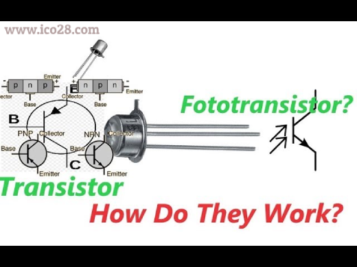
I. Introduction
A PNP transistor, a basic component in electronics, works based on its extraordinary structure and guidelines of operation. Unlike its NPN partner, a PNP transistor comprises three semiconductor layers: emitter, base, and collector, orchestrated in a specific course of action. Understanding the usefulness of PNP transistors is essential for planning and analyzing electronic circuits, as they play a significant part in intensification, exchanging, and signal dealing with applications. In this article, we dive into the complexities of PNP transistors, investigating their structure, operation, characteristics, and practical applications.
II. Overview of PNP Transistors
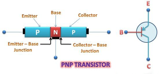
A. Definition and basic structure
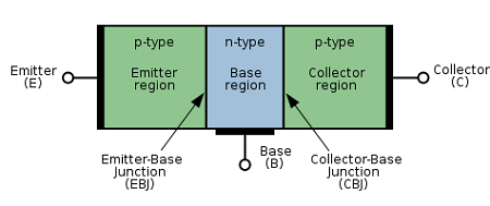
PNP transistors are a kind of bipolar crossing point transistor( BJT) with three layers of semiconductor texture: the emitter, base, and collector. In a PNP transistor, the bigger charge carriers are holes, which sluice from the emitter to the base and, at that point, to the collector. The introductory structure consists of two layers of P-type semiconductor stuffing and a subcaste of N-type semiconductor.
B. Comparison with NPN transistors
Comparing PNP transistors with NPN transistors uncovers crucial contrasts in their operation. Though PNP transistors have a P-type semiconductor subcaste as the captain’s share charge carrier, NPN transistors have an N-type semiconductor subcaste as the bigger portion charge carrier. In NPN transistors, electrons are the larger part carriers, discovering from the emitter to the collector through the base. In showing misprision toward their abecedarian and functional contrasts, both PNP and NPN transistors play abecedarian corridors in electronic circuits.
III. How PNP Transistors Work
A. Description of the three regions: emitter, base, and collector
The PNP transistor consists of three fundamental locales: the emitter, base, and collector. The emitter emanates larger charge carriers (gaps) into the base locale, whereas the collector collects these charge carriers. The base region acts as a control terminal, controlling the stream of charge carriers between the emitter and collector.
B. Clarification of the PNP transistor’s operation principles
The operation of a PNP transistor is based on the rule of minority carrier infusion. When a positive voltage is connected to the base relative to the emitter, it makes a forward inclination, permitting a little current to stream from the emitter to the base. This current controls the bigger current streaming from the emitter to the collector, successfully opening up the signal.
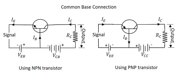
C. Part of biasing and current flow
Biasing plays a vital role in controlling the stream of current through a PNP transistor. By applying the fitting voltage to the base with regard to the emitter, the transistor can be one-sided into either the dynamic, cutoff, or immersion locales. The heading of the current stream from the emitter to the collector is decided by the biasing arrangement, whether it’s forward or inverted one-sided. Appropriate biasing guarantees ideal transistor execution and usefulness in electronic circuits.
IV. Key Characteristics and Applications
A. Voltage and current ratings
PNP transistors, like all electronic factors, have specific voltage and current conditions pivotal for their proper operation within a circuit. These conditions generally include parameters such as maximum collector-emitter voltage( VCEO) and collector current( IC). Understanding these conditions is vital to ensuring the transistor’s life and trustability in a given operation. Deviating from specified conditions can lead to unseasonable failure or erratic behavior of the transistor.
B. Common uses in electronic circuits
PNP transistors find wide use in colorful electronic circuits due to their protean characteristics. They’re generally employed in modification circuits, where they serve as signal amplifiers or switches. Also, PNP transistors are integral factors in voltage controllers, oscillators, and power operation circuits. Their capability to control the current inflow and amplify signals makes them necessary in ultramodern electronics, ranging from audio amplifiers to power force units.
C. Advantages and disadvantages compared to other transistor types
When compared to other transistor types, such as NPN transistors and MOSFETs, PNP transistors offer distinct advantages and disadvantages. One advantage is their compatibility with positive ground systems, making them suitable for specific applications where this configuration is preferred. However, PNP transistors typically have lower current gain and slower switching speeds compared to NPN transistors, limiting their suitability for high-frequency applications. Additionally, their minority carrier conductivity introduces higher power dissipation, resulting in reduced efficiency in certain circuit designs. Understanding these trade-offs is essential for selecting the most appropriate transistor type for a given application.
V. Practical Examples and Circuits
A. Simple PNP transistor configurations
PNP transistors find application in various circuit configurations, ranging from basic to complex. One common setup is the emitter-follower configuration, where the emitter is connected directly to the input signal source, providing high input impedance and low output impedance. Another simple configuration is the common-emitter amplifier, where the input signal is applied to the base and the amplified output is taken from the collector. These configurations illustrate the versatility of PNP transistors in different circuit designs.
B. Analysis of transistor behavior in various circuit setups
Analyzing the behavior of PNP transistors in various circuit setups offers valuable insights into their operation and performance characteristics. In emitter-follower configurations, PNP transistors exhibit unity gain, providing voltage buffering and impedance matching between stages of a circuit. In common-emitter amplifiers, PNP transistors amplify the input signal with a phase inversion, making them suitable for applications requiring signal amplification and inversion. Understanding the behavior of PNP transistors in these setups is essential for designing and troubleshooting electronic circuits effectively.
![]()
VI. Conclusion
In conclusion, digging into the complexities of PNP transistor functionality gives profitable insights into their significant role in advanced electronics. By understanding the operation standards and key characteristics of PNP transistors, engineers and enthusiasts alike can effectively use their capabilities in different applications. Through viable illustrations and circuit examination, we have explained the significance of PNP transistors in forming electronic systems’ behavior. Moreover, investigating procedures and contemplations underscores the significance of maintaining ideal execution. Overall, grasping the subtleties of PNP transistors engages people to design, troubleshoot, and improve with certainty in the energetic field of electronics.